Resistors(Network) | Chip Resistor Networks
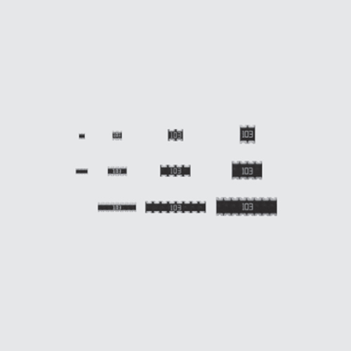
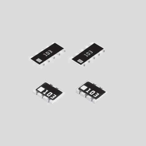
Chip Networks (Concave Termination) CN

 CN.pdf CN.pdf
|
Chip Networks (Concave Termination) CN
Features More advancement in the mounting density than individual chip resistors. Mounting cost reduction by decreasing the number of parts mounting times. 2, 4 and 8 elements of SMD resistor arrays are available. Precision type ��1% is available. Higher self-alignment effect in reflow-soldering process. Suitable for an image recognition mounter due to square corner design. Suitable for both reflow and flow solderings. Products with lead free termination meet EU-RoHS requirements. EU-RoHS regulation is not intended for Pb-glass contained in electrode, resistor element and glass. AEC-Q200 Qualified(CN1J4)
Applications Resistors for Damping, Pull-up/Pull-down, Termination for digital circuits. LED current limiting. Terminals for SDRAM, DRDRAM. (1 - 10��, 5% available)
|
cn_a.pdf
|
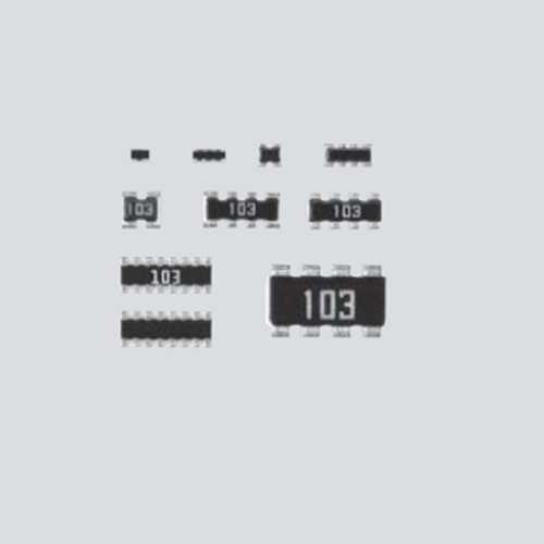
Chip Networks CN-A/CN-K
Features More advancement in the mounting density than individual chip resistors. Mounting cost reduction by decreasing the number of parts mounting times. Easy soldering fillet inspection. 2, 4 and 8 elements of SMD resistor arrays are available. Precision type ��1% is available. Suitable for an image recognition mounter due to square corner design. (CN-K type) Suitable for both flow and reflow soldering. Products with lead free termination meet EU-RoHS requirements. EU-RoHS regulation is not intended for Pb-glass contained in electrode, resistor element and glass. AEC-Q200 Qualified (CN1E4K, CN1J4A, CN1J4K).
Applications
|
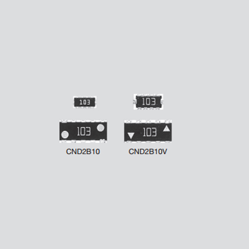
Chip Networks (Concave Termination) CND
CND.pdf
|
Chip Networks (Concave Termination) CND
Features
More advancement in the mounting density than individual chip resistors. Mounting cost reduction by decreasing the number of parts mounting times. Higher self-alignment effect in reflow-soldering process. Suitable for an image recognition mounter due to square corner design. Suitable for both reflow and flow solderings. Integrated 8 elements for Pull-up/Pull-down. Products with lead free termination meet EU-RoHS requirements. EU-RoHS regulation is not intended for Pb-glass contained in electrode, resistor element and glass.
Applications
|
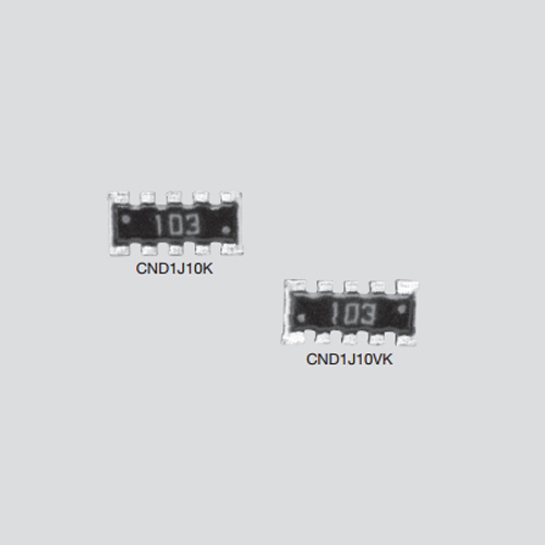
Chip Networks (Convex Termination) CND-K
cnd_k.pdf
|
Chip Networks (Convex Termination) CND-K
Features More advancement in the mounting density than individual chip resistors. Mounting cost reduction by decreasing the number of parts mounting times. Easy soldering fillet inspection. Suitable for an image recognition mounter due to square corner design. Suitable for both flow and reflow soldering. Integrated 8 elements for Pull-up/Pull-down. Products with lead free termination meet EU-RoHS requirements. EU-RoHS regulation is not intended for Pb-glass contained in electrode, resistor element and glass.
Applications
|
Chip Networks (Concave Termination) CNB
CNB.pdf
|
Chip Networks (Concave Termination) CNB
Features More advancement in the mounting density than individual chip resistors. Mounting cost reduction by decreasing the number of parts mounting times. Higher self-alignment effect in reflow-soldering process. Suitable for an image recognition mounter due to square corner design. Suitable for both reflow and flow solderings. 4 or 8 elements are integrated for Pull-up/ Pull-down. Easy to make a PWB layout with a zigzag electrode. Products with lead free termination meet EU-RoHS requirements. EU-RoHS regulation is not intended for Pb-glass contained in electrode, resistor element and glass.
Applications
|
BR.pdf
|
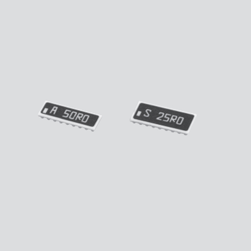
BGA Resistor Networks BR
Features This BGA packaging resistor network device virtually eliminates channel capacitance, a primary cause of reduced system performance. This device eases routing design of DDR SDRAM termination. Higher integration of resistor elements saves overall assembly costs. Lead free terminal. High precision ��1% is standard. BGA packaging is effective in a saving of the board space and high density mounting. Products meet EU-RoHS requirements. EU-RoHS reguation is not intended for Pb-glass contained in electrode, resistor and glass.
|